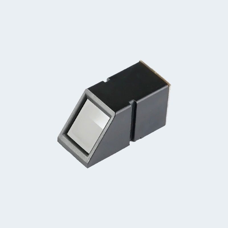
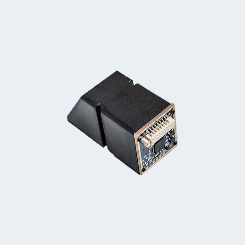
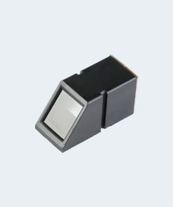
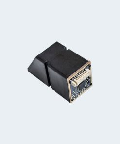
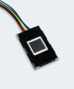
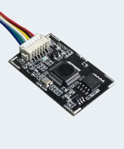
AS606 optical fingerprint sensor JM-101B fingerprint matching fingerprint sensor module
|
Serial number |
Pin description | Note |
|
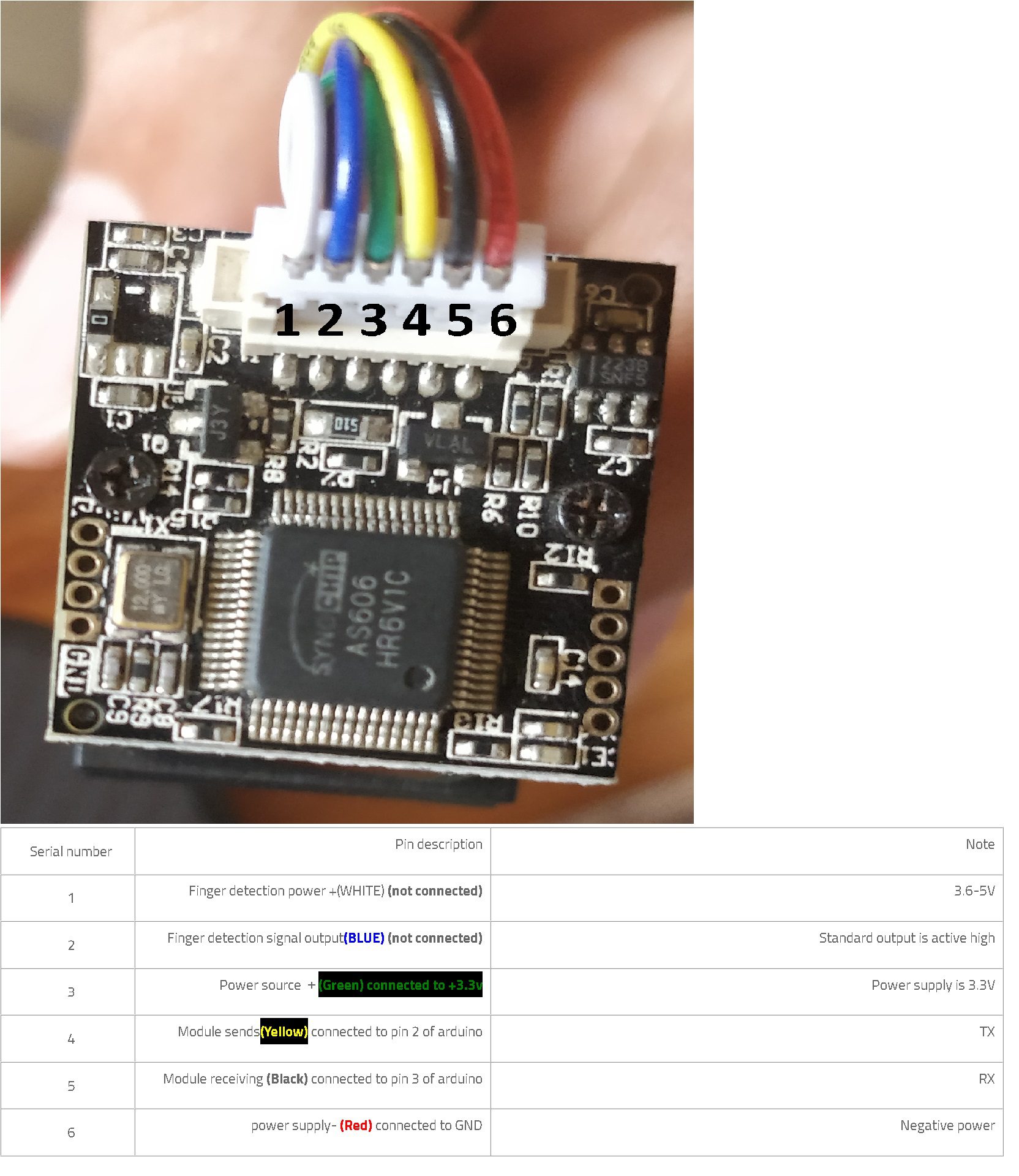
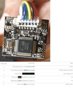
1 |
Finger detection power +(WHITE) (not connected) | 3.6-5V |
|
2 |
Finger detection signal output(BLUE) (not connected) | Standard output is active high |
|
3 |
Power source +(Green) connected to +3.3v | Power supply is 3.3V |
|
4 |
Module sends(Yellow) connected to pin 2 of arduino | TX |
|
5 |
Module receiving (Black) connected to pin 3 of arduino | RX |
|
6 |
power supply- (Red) connected to GND | Negative power |
use Adafruit library examples (Enroll and Fingerprint)
1 , the working principle ,
The fingerprint processing includes two processes: the fingerprint login process and the fingerprint matching process [where the fingerprint matching is divided into two ways : fingerprint comparison ( 1: 1 ) and fingerprint search ( 1: N )].
When the fingerprint logon, a fingerprint entry for every 2 times to 2 times the input image processing, synthetic templates stored in the module. During fingerprint matching, the fingerprint image is input and processed through the fingerprint head sensor, and then compared with the fingerprint template in the module (if matched with a template specified in the module, it is called fingerprint comparison mode, that is 1: 1 way; if matching with multiple templates, it is called fingerprint search mode, ie 1: N mode), the module gives the matching result (pass or fail).
2 , the technical parameters
Feature file: 256 bytes
Template file: 512 bytes
Supply voltage: DC 3V
Supply current: Working current: < 120mA Peak current: < 130mA
Fingerprint image entry time: <0.5 seconds
Window area: 18.5mm X 14.6mm
Matching method: comparison method (1: 1)
Search method (1: N)
Storage capacity: 200 Mei
Security level: five levels (low to high: 1, 2, 3, 4, 5) system default 3
False acceptance rate (FAR): <0.001% (when the security level is 3)
Rejection rate (FRR): <1.0% (when the security level is 3)
Search time: <1.0 second (1: 500 hour average)
Resolution: 500dpi
Host computer interface: UART (TTL logic level)
Communication baud rate (UART): (9600 ╳ N) bps where N = 1 ~ 6 (default value is N = 6, ie 57600bps)
working environment:
Temperature: -25 ℃ - + 55 ℃
Relative humidity: 40% RH to 85% RH (non-condensing)
Storage environment:
Temperature: -40 ℃ - + 85 ℃
Relative humidity: <90% H (non-condensing)
The optical module ( a C3 ) Dimensions (L ╳ W is ╳ H) : length 47.65mmX width 20.50mmX high21.20mm
Semiconductor module dimensions (L ╳ W ╳ H) :
Capacitive module Dimensions: Main control board: Length 35mm X width 28mm X height 7mm
Sensor: Long 33.4mmX width 20.4mm
Scraping module dimensions: main control board: length 35mm X width 28mm X height 7mm
Sensor board: length 24mmX width 20mmX height 5mm
Chapter III Hardware Interface
3.1 Host computer interface (labeled on the board: J1 )
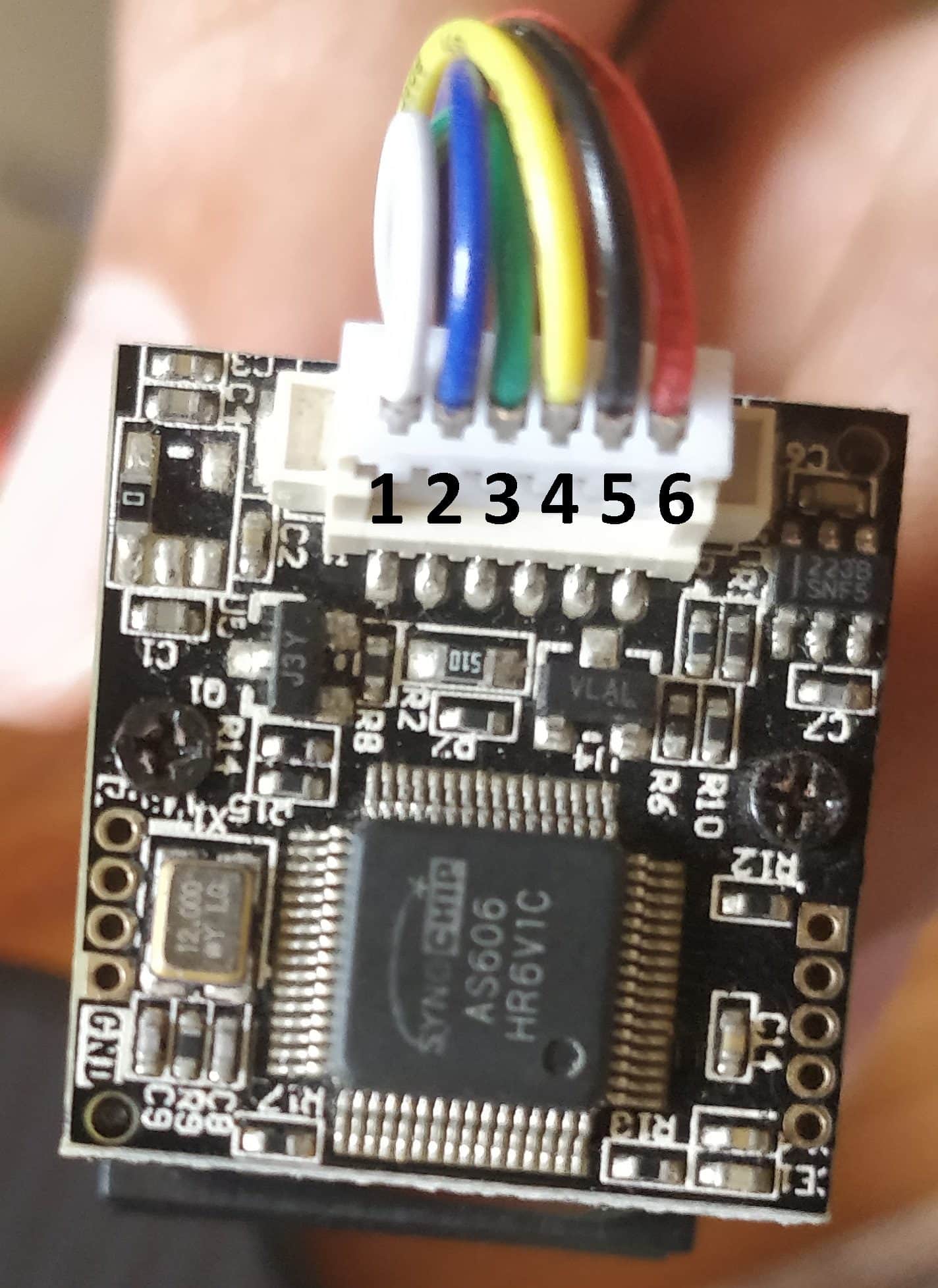
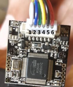
The module and the host computer are connected through a 6PIN 1.25mm pitch line. The pins are defined as follows:
|
Serial number |
Pin description | Note |
|
1 |
Finger detection power +(WHITE) (not connected) | 3.6-5V |
|
2 |
Finger detection signal output(BLUE) (not connected) | Standard output is active high |
|
3 |
Power source +(Green) connected to +3.3v | Power supply is 3.3V |
|
4 |
Module sends(Yellow) connected to pin 2 | TX |
|
5 |
Module receiving (Black) connected to pin 3 | RX |
|
6 |
power supply- (Red) connected to GND | Negative power |
The module requires two sets of power to supply power separately, one for the serial port power of the module, and one for the power chip power supply, which share the ground.
1 and 6 are the power supply of the sensor chip and need to be powered all the time; 3 and 6 are the serial power supply of the module. When the finger is close to the fingerprint window, pin 2 generates a high level. When the customer MCU receives this level, the module 3 and 4 pins are powered on through the module serial port power control circuit (transistor or MOS tube) .
3.1.1 Serial communication
When the module communicates with user equipment, the J1 pin of the interface is defined as follows:
|
Pin number |
name |
Types of |
Function description |
|
1 |
+ 3.3V_ON |
In |
Finger detection power input |
|
2 |
TOUCH |
Out |
Finger detection signal output |
|
3 |
VUSB |
in | Positive power input. (Thread color: red) |
|
4 |
TX |
out |
Serial data output. TTL logic level. (Thread color: green) |
|
5 |
RX |
in |
Serial data input. TTL logic level. (Thread color: white) |
|
6 |
GND |
– |
Signal ground. Internally connected to power ground. (Thread color: black) |
Note: In the type column, in means input to the module, and out outputs from the module.
3.1.1.1 Hardware connection
Module through the serial communication interface, can be employed directly with 3.3V or 5V microcontroller communication: data transmission module foot ( 4 feet the TX ) data receiving end connected to bit machine ( the RXD ) , the module data receiving pin ( 5 feet the RX ) connected Data sending end of the host computer ( TXD ).
If you need to communicate with the host computer with RS-232 level (for example: PC ), please add level conversion circuit (for example: MAX232 circuit) between the module and the host computer .
3.1.1.2 Serial Protocol
Adopt half-duplex asynchronous serial communication. The default baud rate is 57600bps , which can be set to 9600 to 115200bps through commands .
The transmitted frame format is 10 bits, a 0 -level start bit, 8 -bit data (lower bit first) and a stop bit, no parity bit.
3.1.1.3 Power-on delay time
After the module is powered on, it takes about 200mS for initialization. During this period, the module cannot respond to commands from the host computer.
3.1.1.4 Electrical parameters ( all levels are referenced to the power / signal ground GND )
1. Power Input
|
Term project |
Reference number |
unit |
Preparation Note |
||
|
Smallest |
typical |
maximum |
|||
|
Supply voltageVin |
3.8 |
5 |
6 |
V |
Normal working value |
|
Limit voltage Vin max |
– 0.3 |
|
6 |
V |
Exceeding this range may cause permanent damage |
|
Working currentIcc |
90 |
100 |
110 |
mA |
|
|
Peak currentIpeak |
|
150 |
mA |
|
|
2. TXD (output, TTL logic level)
|
project |
Article pieces |
Reference number |
unit |
Note |
||
|
Smallest |
typical |
maximum |
||||
|
V OL |
I OL = - 4mA |
|
0.4 |
V | Logic 0 | |
|
V OH |
I OH = 4mA |
2.4 |
3.3 |
V |
Logic 1 | |
3. RXD pin (input, TTL logic level)
|
project |
Article pieces |
Reference number |
unit |
Note |
||
|
Smallest |
typical |
maximum |
||||
|
V IL |
|
0.6 | V | Logic 0 | ||
|
V IH |
|
2.4 |
V |
Logic 1 | ||
|
I IH |
V IH = 5V |
|
1 |
|
mA | |
| V IH = 3.3V |
|
30 |
|
uA | ||
|
V Imax |
– 0.3 |
5.5 | V | Limit input voltage | ||
3.1.2 USB communication
Module and the user equipment USB when communication interface USB labeled foot is defined as follows:
|
Pin number |
name |
Types of |
Function description |
|
1 |
VCC |
in | Positive power input. (See 3.1.1.4 for electrical parameters) |
|
2 |
D- (DM) |
In / Out |
USB data cable. |
|
3 |
D + (DP) |
In / Out |
USB data cable. |
|
4 |
GND |
– |
Signal ground. Internally connected to power ground. |
Note: In the type column, in means input to the module, and out outputs from the module.
The first pin near the crystal is the first pin
3.2 sensor interface (labeled on the board: J1 )
As shown in the figure below, the sensor interface uses a 6P — 1.25 pitch seat, and a 6P — 15mm connection cable is used.
In order to meet the needs of different customers, the module system provides a lot of resources for users to use.
4.1 buffer
There is an image buffer ImageBuffer and two 512-byte feature file buffers CharBuffer1 and CharBuffer2 in the module RAM. The user can read and write any buffer through instructions. The contents of the image buffer and the two feature file buffers are not saved when the module is powered off.
4.1.1 Image buffer
The image buffer ImageBuffer is used to store image data and the internal image processing of the module. When uploading / downloading images, the image format is 256 ╳ 288 pixels.
In order to speed up when uploading or downloading images through the UART port, only the upper four bits of the pixel byte are used, that is, 16 levels of gray are used, and each byte represents two pixels (the upper four bits are one pixel and the lower four bits are the same One pixel in the next column of the row, that is, two pixels are combined into one byte and transmitted ). Because the image has 16 gray levels, when uploading it to a PC for display (corresponding to the BMP format), the gray level should be extended (extended to 256 gray levels, that is, 8 -bit bitmap format).
Transmission through the USB port is an entire 8-bit pixel, that is, 256 gray levels.
4.1.2 Feature file buffer
The feature file buffer CharBuffer1 or CharBuffer2 can be used to store both ordinary feature files and template feature files.
4.2 Fingerprint library
The module has opened up a section of storage area in FLASH as a storage area for fingerprint templates, commonly known as a fingerprint database. The data in the fingerprint database is protected by power failure.
The fingerprint template is stored according to the serial number. If the capacity of the fingerprint database is N, the serial number of the fingerprint template in the fingerprint database is defined as: 0, 1, 2 … N-2, N-1. Users can only access the contents of the fingerprint database based on the serial number.
4.3 System configuration parameters
In order to facilitate the use of the user, the module opens some system parameters, allowing the user to modify the specified parameter value (by the parameter number) individually through instructions. See setting the basic parameters of the system module commands SetSysPara and the system parameter command ReadSysPara .
When the host computer sends a command to modify the system parameters, the module responds according to the original configuration. After the response, the system settings are modified and the configuration is recorded in FLASH. After the system is powered on next time, it will work according to the new configuration.
4.3.1 Baud rate control (parameter number: 4 )
This parameter controls the communication baud rate when the module communicates with the host computer through UART. If the parameter value is N (N ranges from 1 to 12), the corresponding baud rate is (9600 ╳ N) bps .
4.3.2 Security level (parameter number: 5)
This parameter controls the search fingerprint matching and match threshold, points of 5 , ranging as follows: 1 , 2 , 3 , 4 , 5 .
When the security level is 1, the false acceptance rate is the highest and the rejection rate is the lowest. When the security level is 5 , the false acceptance rate is the lowest and the rejection rate is the highest.
4.3.3 Package Content Length (Parameter Number: 6)
This parameter controls the maximum length of the packet content allowed in the data when communicating with the host computer. The value ranges from 0, 1 , 2 , and 3. The corresponding lengths (bytes) are: 32 , 64 , 128 , 256 .
4.4 System Status Register
The system status register indicates the current working status of the module. It can be read by the ReadSysPara instruction, and the length is 1Word.
Its definitions are as follows:
|
Tag number |
15 4 |
3 |
2 |
1 |
0 |
|
significance |
Reserved |
ImgBufStat |
PWD |
Pass |
Busy |
Note:
L the Busy : one bit, set to 1 indicates that the system is executing a command, 0 indicates the system is idle;
l Pass : 1 bit, set to 1 to indicate that the fingerprint verification is passed;
l PWD : One bit. Set to 1 to indicate that the device handshake password passes verification.
l ImgBufStat : One bit. Set to 1 to indicate that there is a valid fingerprint image in the fingerprint image buffer.
4.5 Module Password
After the module is powered on and reset, it will first check whether the device handshake password is modified. If it has not been modified, the module considers that the upper computer has no need to verify the password and directly enters the normal working state; that is, when the module password is the default password, the password may not be verified. Password is 4 bytes , the factory default ports make is: 0x00000000 .
If the module’s internal password has been modified (see SetPwd ), the device handshake password must be verified first, and the module will enter the normal working state after the password is passed. Otherwise the module refuses to execute any instructions.
After the password is changed, the new password is saved in Flash, and it is still saved after power failure.
See the verify password VfyPwd instruction and the set password SetPwd instruction.
4.6 Module address
Each module has an identification address. When the module communicates with the host computer, each instruction / data is transmitted in the form of a data packet. Each data packet contains an address and an address item. The module only responds to instructions and data packets containing the same address as itself.
The module address is 4 bytes. The factory default value is 0xFFFFFFFF. The user can modify the module address by instructions (see Set Module Address Instruction SetAdder). After the module address is modified, the new address is still saved after the module is powered off.
4.7 Random Number Generator
Integrated module internal hardware random number generator 32 (random number seed not required), the user can make an instruction module generates a random number and upload, see sampling a random number of instructions GetRandomCode .
Related products
All Electronics Components
All Electronics Components
All Electronics Components
All Electronics Components
All Electronics Components
All Electronics Components
All Electronics Components
All Electronics Components


